Programming Tenstorrent processors
This post was going to be my rewrite of the original Tenstorrent Programming Model document, which is in their repo since ages but never completed. But decided against it as it's too market-y and not my usual (often brutally) honest style. This post was also going to just be an introduction. But ended up as a "here's how to use the processor and where footguns exist" kind of post.
Readers of this post are assumed to have a solid understanding of computer architecture at an undergraduate level, as well as familiarity with parallel programming models and GPU/AI accelerator basics.
Tenstorrent Architecture Overview
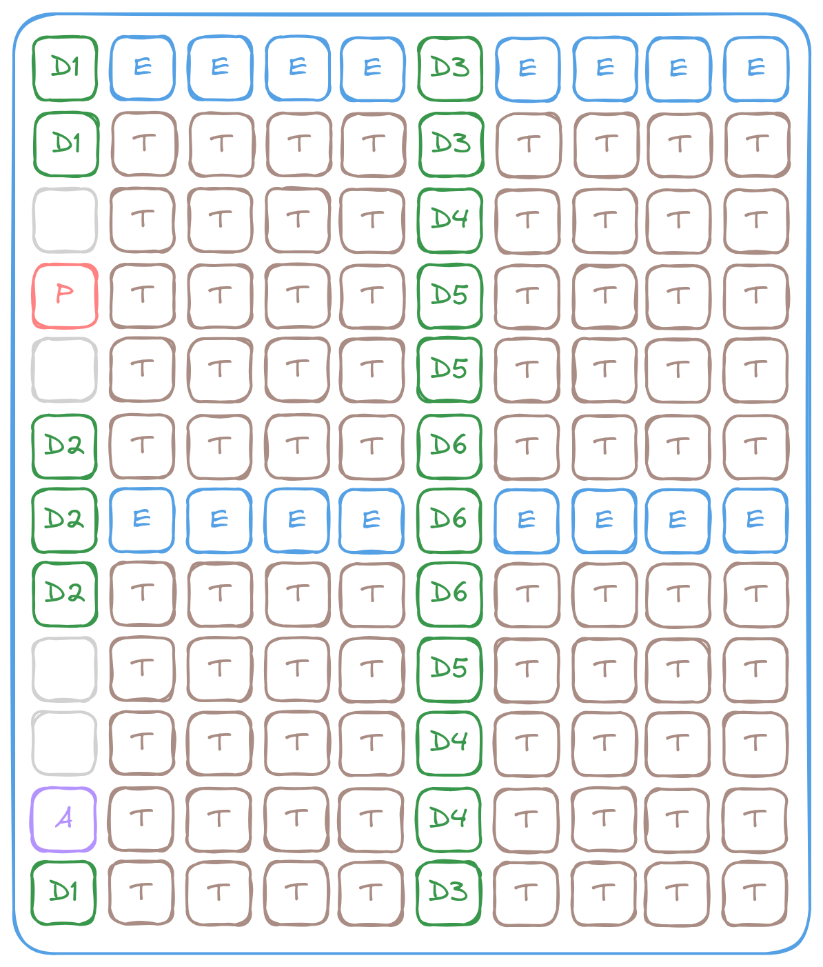
The Tenstorrent architecture is a different kind of AI processor. Unlike GPUs where you get a massive core count and parallelize across thousands of cores (not really, SIMT is a lie that the compiler told you). Tenstorrent chips are a grid of different nodes. Most are compute elements called a Tensix core ("core" is overloaded in computer architecture, bear with me) sprinkled with some memory, chip management and Ethernet nodes to facilitate the computation.
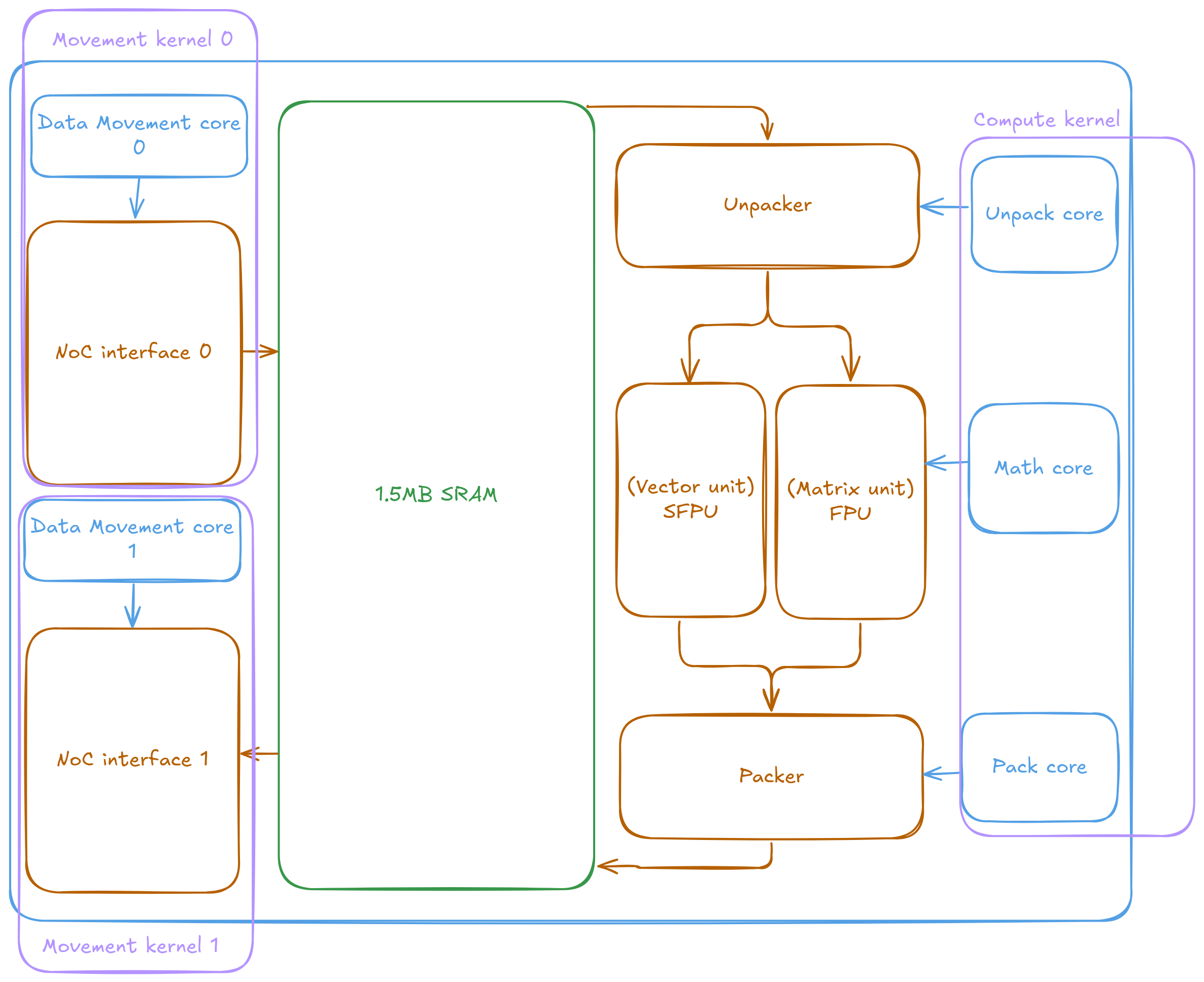
Each Tensix contains 5 "Baby" RISC-V CPUs, 2 NoC interfaces, a vector unit, a matrix/tensor unit and a pack and unpacker, as well as 1.5MB of SRAM so stuff can be stored and facilitates data exchange between local components. See the following diagram for a rough idea of the Tensix.
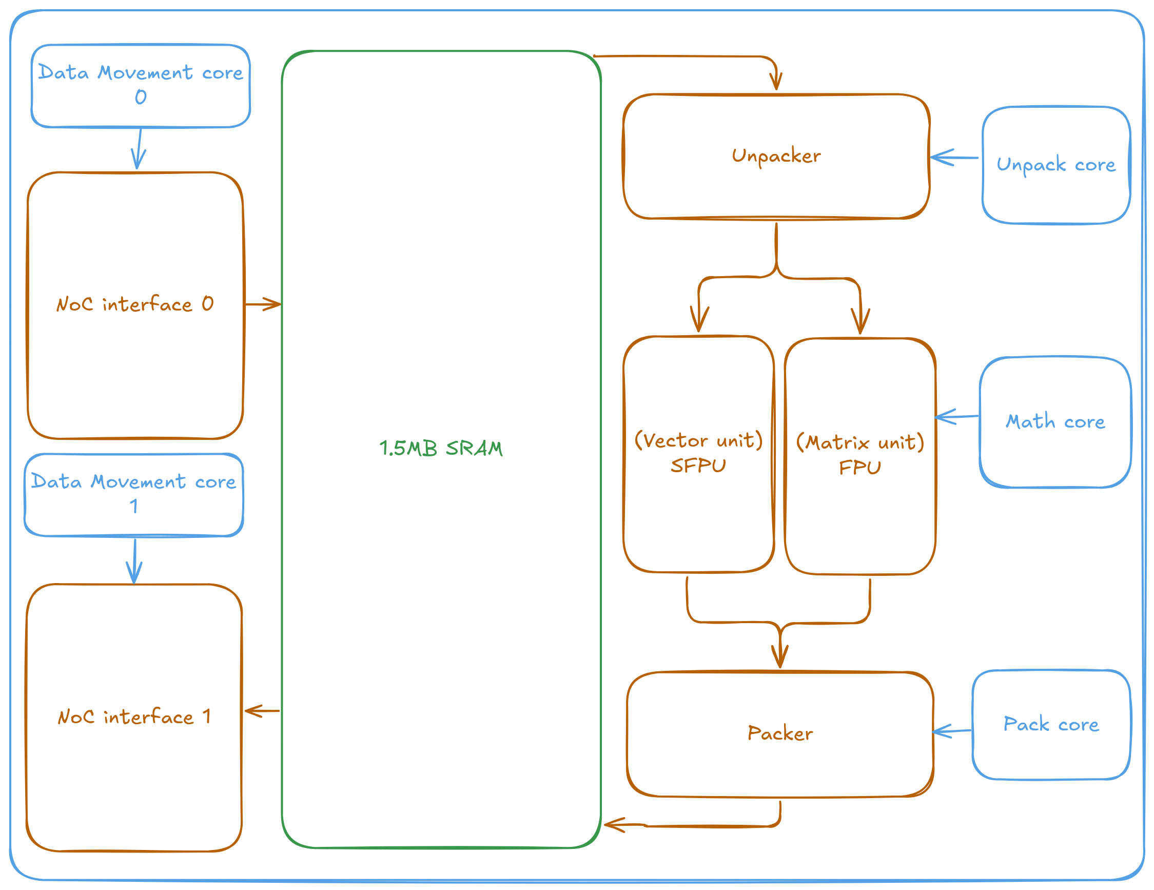
It's a lot to take in. Let's start from the obvious - RISC-V cores and the SRAM. The SRAM as expected stores data local to the Tensix and feeds the compute engines/peripherals. Unlike GPUs, where the Warp/Compute Unit (CUDA/OpenCL terms) supplies the majority of computation power, the Baby RISC-V cores in Tensix primarily handle instruction dispatch. The Baby RISC-V cores does not involve itself in the actual computation, instead they simply dispatch instructions to the NoC/Matrix/Vector/{,Un}packer units that gets the real work done. They are called "Baby" cores for a reason - they are really, really small. Think like your textbook 5 stage pipelined, single issue, basic branch prediction and async loading. That's it.
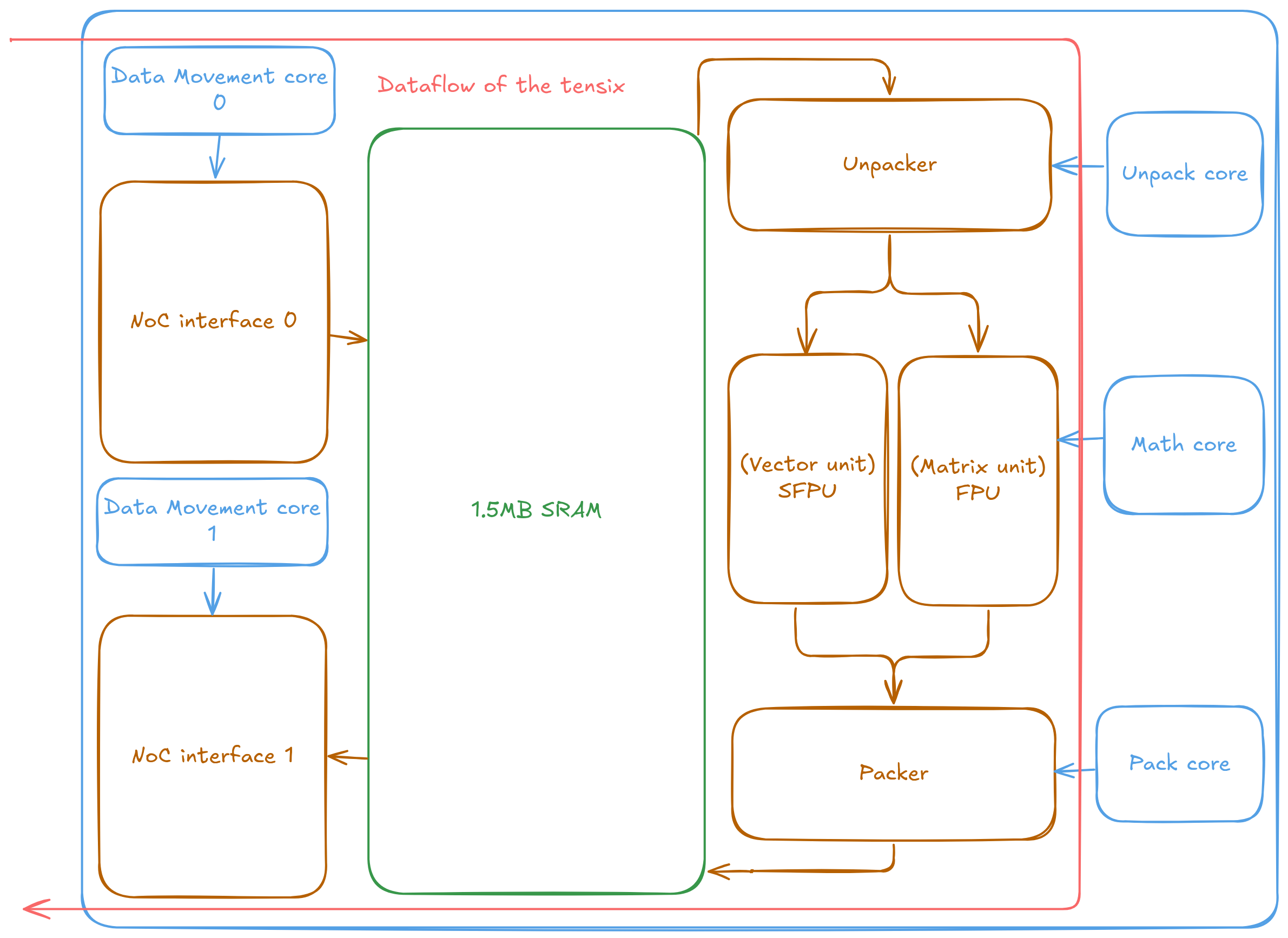
The intended data flow is as follows, resembling software pipelining but on a distributed and hardware scale:
- NoC 0 reads data from DRAM (or accept data from other Tensixes)
- Unpacker unpacks the data into a format that can be processed by the matrix/tensor unit
- Matrix/tensor unit performs the computation
- Packer packs the result back into a format for storage
- NoC 1 sends the result to DRAM (or other Tensixes)
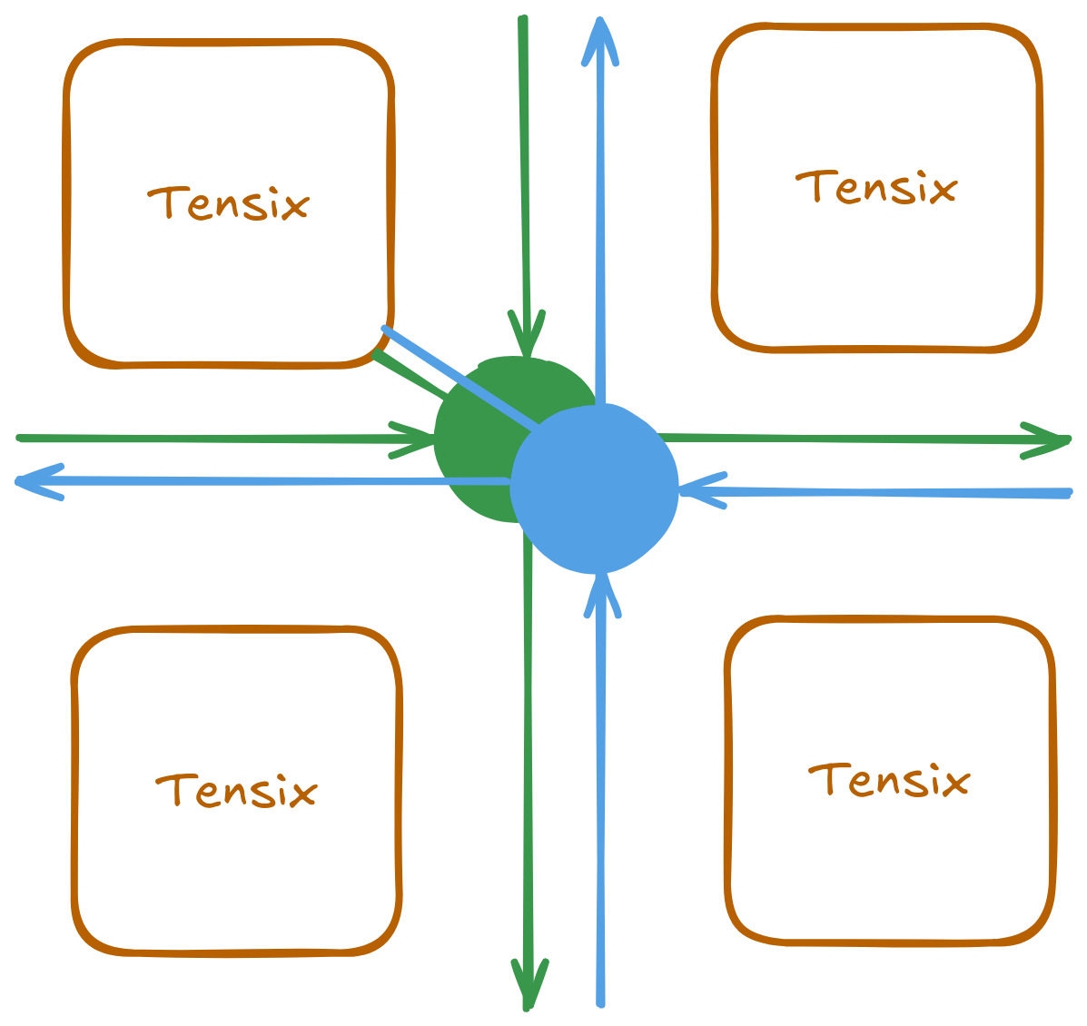
As a matter of fact, the NoCs are full-duplex-ish. They are unidirectional and wraps around the chip, with NoC 0 running in the opposite direction of NoC 1. However both NoCs supports sending and receiving data at the same time. The unidirectional design of the NoCs reduces power consumption and area usage, while the wraparound (2D torus) topology ensures that every point on the chip remains accessible from every other point. Additionally, having both NoCs run in opposite directions naturally provides a return path after each operation.
It is important to understand that the flow described above is just one possible configuration. The RISC-V cores are fully in control of what every part of the Tensix is doing. For complex operations, it is totally doable (and sometimes do in production) to intentionally play tricks to gain double the effective NoC bandwidth by simultaneously using both interfaces for reading data, at the cost of not able to overlap reads and writes together. Or use the SRAM as a temporary storage for intermediate results within the operation itself.
Even though the chip looks like a systolic array. Flexibility is paramount. There is no one stopping you from using it like a CPU with a SPMD pattern. In fact SPMD is the default pattern outside of operations that can take advantage of physical topology (ex: the efficient Scaled Dot Product Attention algorithm on Wormhole).
It looks like a single operation is 5 programs that developers need to write, no? No, unless if you hell bent to. The 2 data movement kernels can be developed separately and independently. And often reused across different operations. Instead of the traditional parallel approach to utilize multiple cores, The 3 compute cores work cooperatively to perform the computation.
How do these three kernels synchronize with each other? How does the compute kernel know when data is ready, and how does the writer know when computation is complete and results can be safely stored? Tenstorrent implements this through circular buffers backed by hardware mutexes and SRAM. While circular buffers are the implementation detail, conceptually they function as pipes or queues. Kernels can wait for available space in the pipe, write data to it, and then mark that data as ready. Similarly, they can wait for data to become available from the pipe before processing it.
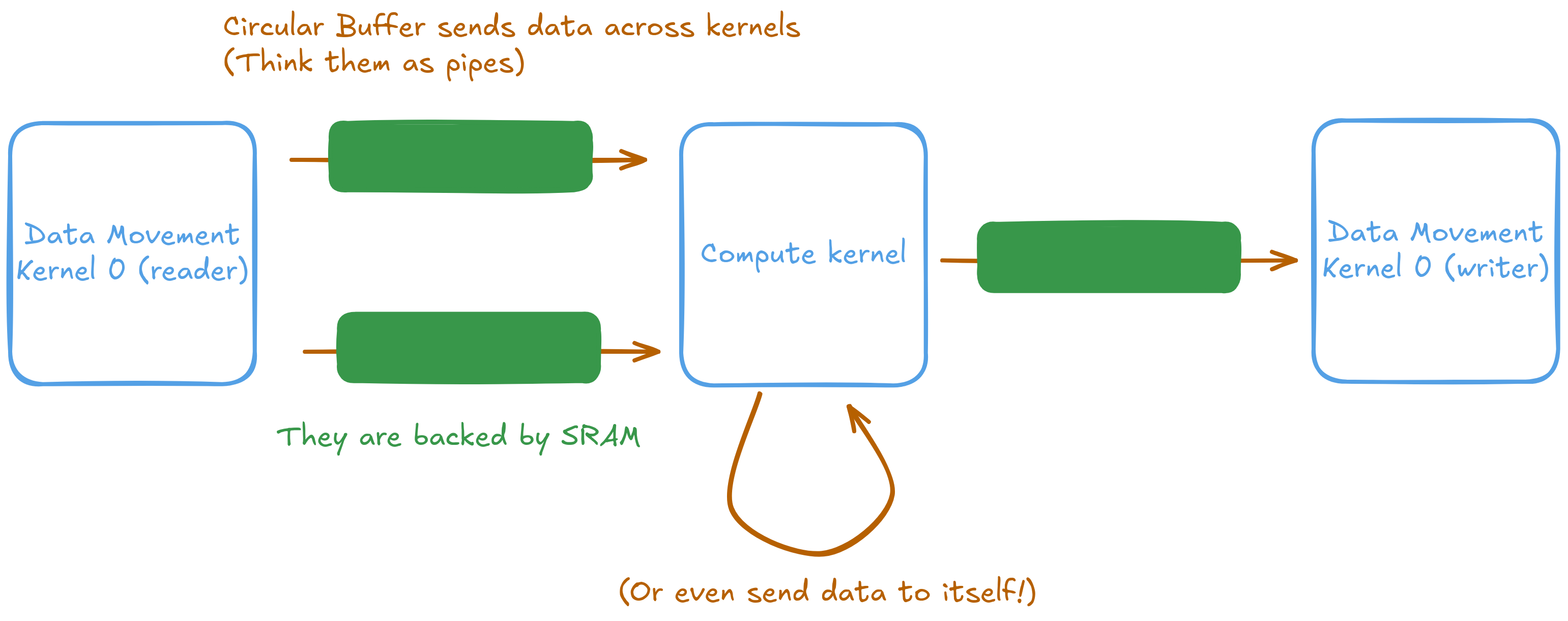
Hopefully with the above information, it is easy to understand how vector addition is performed. There are 3 written kernels. The reader, the writer, and the compute kernel. The react accepts 3 parameters. Address of A and B, and the number of tiles to process. The compute kernel waits data to be made available by the reader, performs add. Then the writer waits for results from the compute kernel, and writes them to the output buffer. As the NoC and computation engines are peripherals. All operations are asynchronous thus fences and barriers are needed to ensure proper synchronization.
The following are the kernels for vector addition on Tenstorrent hardware. I left a lot of details out to keep this introduction concise. So it's ok to be confused.
// data read kernel (data movement kernel 0)
void kernel_main() {
    // Read parameters from the kernel arguments
    uint32_t a_addr = get_arg_val<uint32_t>(0);
    uint32_t b_addr = get_arg_val<uint32_t>(1);
    uint32_t n_tiles = get_arg_val<uint32_t>(2);

    const uint32_t tile_size_bytes = get_tile_size(cb_in0);

    const InterleavedAddrGenFast<true> a = {a_addr, tile_size_bytes, DataFormat::Float16_b};
    const InterleavedAddrGenFast<true> b = {b_addr, tile_size_bytes, DataFormat::Float16_b};

    for (uint32_t i = 0; i < n_tiles; i++) {
        cb_reserve_back(tt::c_1, 1);
        cb_reserve_back(tt::c_0, 1);
        noc_async_read_tile(get_write_ptr(tt::c_0), a, cb_in0_addr);
        noc_async_read_tile(get_write_ptr(tt::c_1), b, cb_in1_addr);

        noc_async_read_barrier();  // Wait until tile reads are done
        cb_push_back(tt::c_0, 1);
        cb_push_back(tt::c_1, 1);
    }
}
Beyond synchronizing with the reader and writer. The compute kernel needs its own synchronization as inernally it is 3 cores running cooperatively. After synchronizing both internally and with the reader and writer, the compute kernel can proceed with actual computation.
// compute kernel
void MAIN {
    uint32_t n_tiles = get_arg_val<uint32_t>(0);
    constexpr uint32_t dst_reg = 0;
    binary_op_init_common(tt::c_0, tt::c_1, tt::c_16);
    add_tiles_init(tt::c_0, tt::c_1);

    for (uint32_t i = 0; i < n_tiles; i++) {
        acquire_dst(); // Make sure we can use the SFPU/FPU registers
        cb_wait_front(tt::c_0, 1); cb_wait_front(tt::c_1, 1); cb_reserve_back(tt::c_16, 1);

        add_tiles(tt::c_0, tt::c_1, 0, 0, dst_reg); pack_tile(dst_reg, tt::c_16);

        cb_push_back(tt::c_16, 1); cb_pop_front(tt::c_0, 1); cb_pop_front(tt::c_1, 1);
        release_dst(); // Release the held register
    }
}
The writer is simple. Just waits for the data to be ready and writes it to the output buffer.
// data write kernel (data movement kernel 1)
void kernel_main() {
    uint32_t c_addr = get_arg_val<uint32_t>(0);
    uint32_t n_tiles = get_arg_val<uint32_t>(1);

    const uint32_t tile_size_bytes = get_tile_size(cb_out0);

    const InterleavedAddrGenFast<true> c = {c_addr, tile_size_bytes, DataFormat::Float16_b};

    for (uint32_t i = 0; i < n_tiles; i++) {
        cb_wait_front(tt::c_16, 1);
        noc_async_write_tile(get_read_ptr(tt::c_16), c, cb_out0_addr);
        noc_async_write_barrier();
        cb_pop_front(tt::c_16, 1);
    }
}
SRAM, interleaved and shared buffers
The massive core count and large SRAM per core enables a new kind of optimization that is impossible on traditional architectures. Unlike crazy pure SRAM-based architectures like Groq or Cerebras, Tensorrent's architecture allows data, intermediate tensor or operator buffers to live in SRAM. This reduces the need for expensive DRAM accesses, especially for small intermediate tensors, leading to performance and power improvements.
This freedom to freely store data on SRAM is powerful. For CPUs and GPUs, operator fusion is almost required to have good performance. As otherwise the intermediate tensors likely won't fit in L2 cache and thus get evicted to DRAM. On Tenstorrent, this is not a problem as data can be stored in SRAM without worrying about eviction. Better, often times the only SRAM needed is local to the core thus maximizing the available bandwidth (NoC bandwidth is no longer a bottleneck).
Likewise, the physical location of the DRAM controllers can be taken advantage of to reduce latency and improve performance. By default "interleaved" mode is used for memory access. This is the most generic mode avaliable and comes with the least downsides. When appropriate, data can be stored in sharded mode. This can reduce the distance and cross talk encountered when accessing DRAM for certain operations. Especially helpful for certain attention and convolution operations.
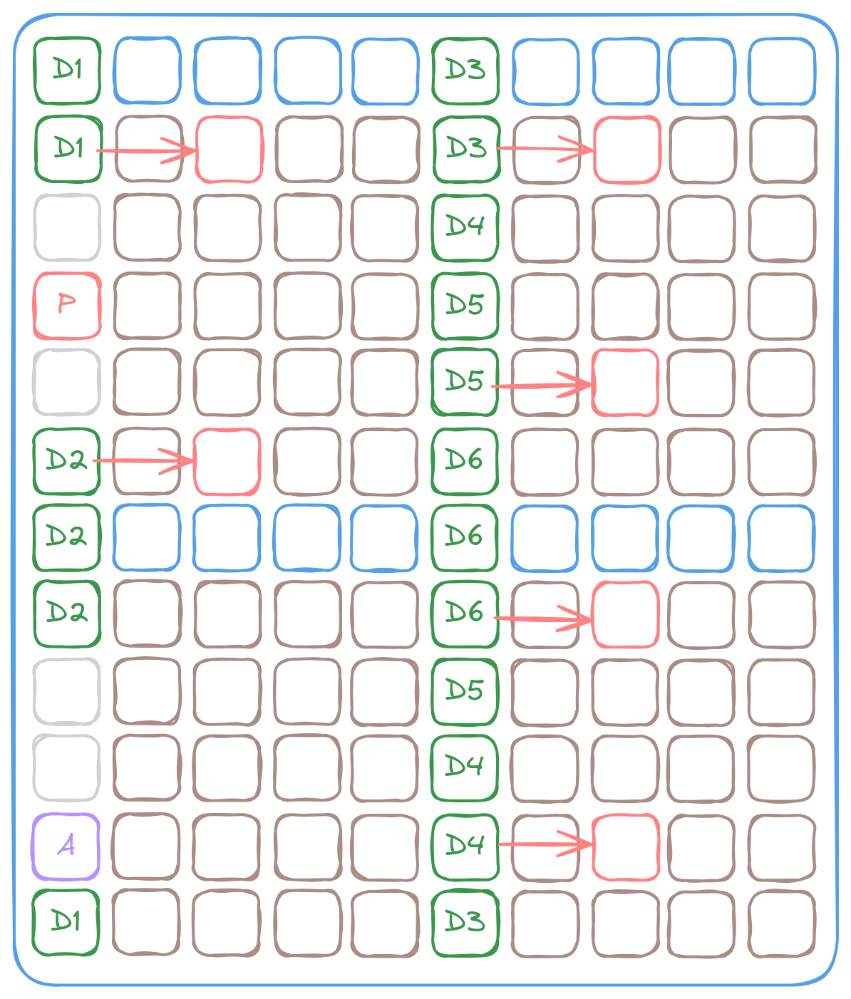
The lack of a linear address space makes many tricks possible. As well as many headaches. See my previous post about how memory works for details.
Native tile based computing
Just like cuTile announced very recently by NVIDIA and used by various Deep Learning Accelerators. The Tensix natively performs operations on 32x32 tiles. This is no coincidence, it's a deliberate design choice to optimize for common operations in deep learning like matrix multiplication and convolution. With tiles, instead of the hardware having to store entire rows of data (often several thousands of elements) as the DMA reads in data linearly, in order to get to the next row for matrix multiplication. a tiled layout switches to the next row every few (in Tenstorrent, it's 32) elements. Vastly increasing the compute-to-SRAM ratio, thus being more efficient.
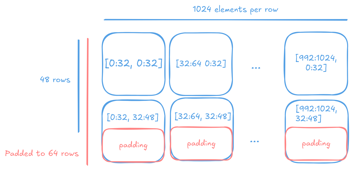
Thus unlike current deep learning frameworks, which use the classic row major layout. Tensors on Tenstorrent devices are tilized for efficient computation. Then untilized when it is needed to be handed back to the traditional realms. Take an 48x1024 matrix for example. Due to the tiles are 32x32, the tilized result is a 64x1024 matrix, with 16 of the 1st dimension being padded.
32x32 tiles are small enough for hardware to digest in a few cycles. Pipeline the computation. And output the result. In an matrix multiplication operation. Instead of CPU/GPUs using tiled access pattern to fuel better cache utilization, thus better performance. This capability is built into the hardware and cost of tilization is amortized over the entire series of operations needed to run deep learning models.
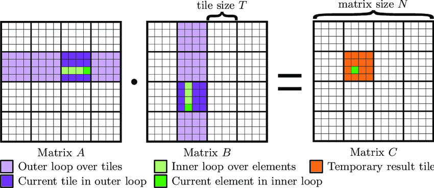
GPUs had a much harder time feeding their tensor cores effectively. They have better vector units to make up for that. But that uses much more power and needs more silicon area. NVIDIA ended up decided they'll have special, tensor aware DMA engines to feed data from DRAM into L1 cache directly.
Where is the cache hierarchy
There is no cache hierarchy on Tenstorrent chips - this is a deliberate design choice. Unlike CPUs and GPUs that rely on complex cache hierarchies to hide memory latency, Tenstorrent provides direct access to SRAM across the entire chip. Every component can access any SRAM on the chip, including the SRAM of other Tensix cores. However, it's crucial to understand that Tensix SRAM is exactly that - SRAM, not cache. This means no automatic caching occurs; data must be explicitly brought into SRAM either by other cores writing to it or by the Tensix itself requesting it. This approach provides deterministic performance and eliminates the unpredictability of cache evictions, but requires developers to be mindful about data movement.
Tenstorrent hardware for GPU experts
Unlike modern GPUs, which rely on a massive number of threads and latency hiding techniques to achieve high throughput, Tenstorrent's hardware takes a different approach. It's designed around asynchronous I/O and efficient resource utilization, even leveraging pipelining for performance. The major differences are as follows
- Each Baby RISC-V in Tensix contains only a single hardware thread
- There is no SIMT architecture disguising SIMD lanes as threads or any latency hiding mechanisms
- Tensix cores use cooperative processing instead of traditional thread scheduling
- The absence of a cache hierarchy results in predictable and consistent memory access latency
- Explicit DMA operations are required to access DRAM
- The NoC interconnect enables efficient near-memory computation
Tenstorrent hardware for CPU experts
Like the IBM CELL processor, each Tensix has dedicated SRAM that the Baby RISC-V cores access directly. Any data not in local SRAM must be explicitly DMA'd into it, either by another core writing to it or by the Tensix requesting it. Each Tensix contains its own vector and matrix units, like modern CPUs. However, the entire chip lacks a cache hierarchy, resulting in predictable and consistent(-ish) latency. When data fits in SRAM, you automatically achieve maximum performance without needing special optimization tricks. And cores within the Tensix work cooperatively instead of each core independently finishing their share of the work.
The Baby RISC-V cores are simple RISC-V 32IM processors that don't support task switching. Since explicit DMA is required to access DRAM (which exists outside the Tensix's address space), there are no memory consistency to manage. Core to core data passing within the Tensix is assisted by hardware mutexes and the circular buffer.
Scaling beyond one chip
As models are getting larger and larger, it is almost a requirement to support multi chip co-processing to be a successful product - to serve state-of-the-art models that are growing in size. The field of Machine Learning used to just rely on the CPU and the PCIe bus to handle data transfers between the computation devices. However, long before Large Language Models (LLMs) became popular, people recognized the true scale of the problem and developed various solutions to address this challenge, often in the form of proprietary data links like NVLink and Infiniband. They work and serve the purpose; however, they are really expensive - not just the cabling, but also the switches needed to connect multiple systems together. What if there's an existing, open standard, widely available, low-cost, high-performance solution that can be used to connect multiple systems together?
Ethernet! NVLink gets up to 50GB/s (400Gbps) with NVLink 5.0. That's rookie numbers (which is yet to be deployed). All the while though cutting edge, 400Gbps Ethernet is and has been widely adopted in data centers and cloud infrastructure (shame Miklroik hasn't put out a 400Gbps or 200Gbps Ethernet switch yet, but that's just me being a Mikrotik fan). To put salt on the NVLink shaped wound, The Tenstorrent chips themselves have enough NoC bandwidth and computing power to act as a switch on its own. While compute is not affected at all. Talk about hyper-convergence!
That gotta be some exotic setup and be super experimental, you say. Experimental, maybe. But exotic, no. the N300 card is a great example of this. It is a PCIe with 2 Wormhole chips directly on the card. The chip connected via PCIe directly to the host is called the L chip - L stands for Local or Left, as it is local to the CPU and on the left of the card - and the other is called the R chip (short for Right or Remote). The SDKs allows developers to treat these chips exactly the same. Be it allocating memory, executing kernels, or even uploading data to the chips.
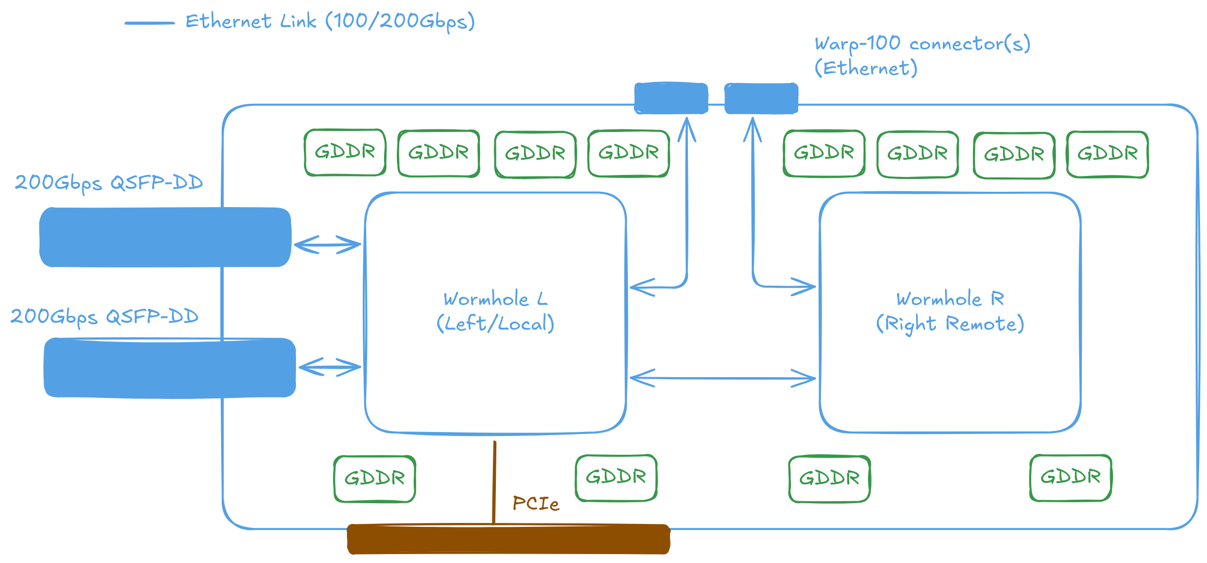
The same scheme can scale well beyond 2 chips. The QuietBox contains 8 Wormhole or 4 Blackhole processors. And forms a mesh of processors. Traffic can be sent and received between processors by writing specialized code that send traffic over the Ethernet links. I have cribbed, cough, borrowed the format from Corix's blog post series on the Tenstorrent Wormhole hardware.
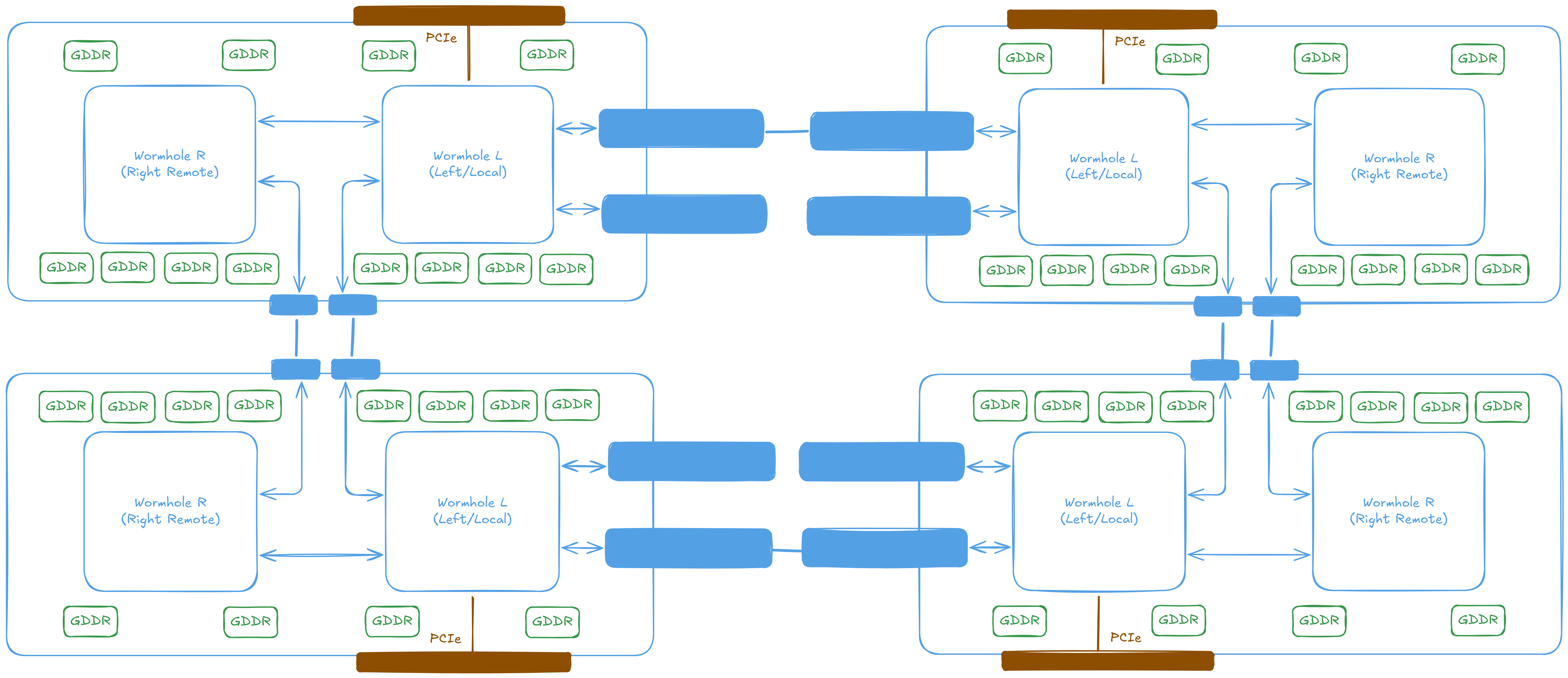
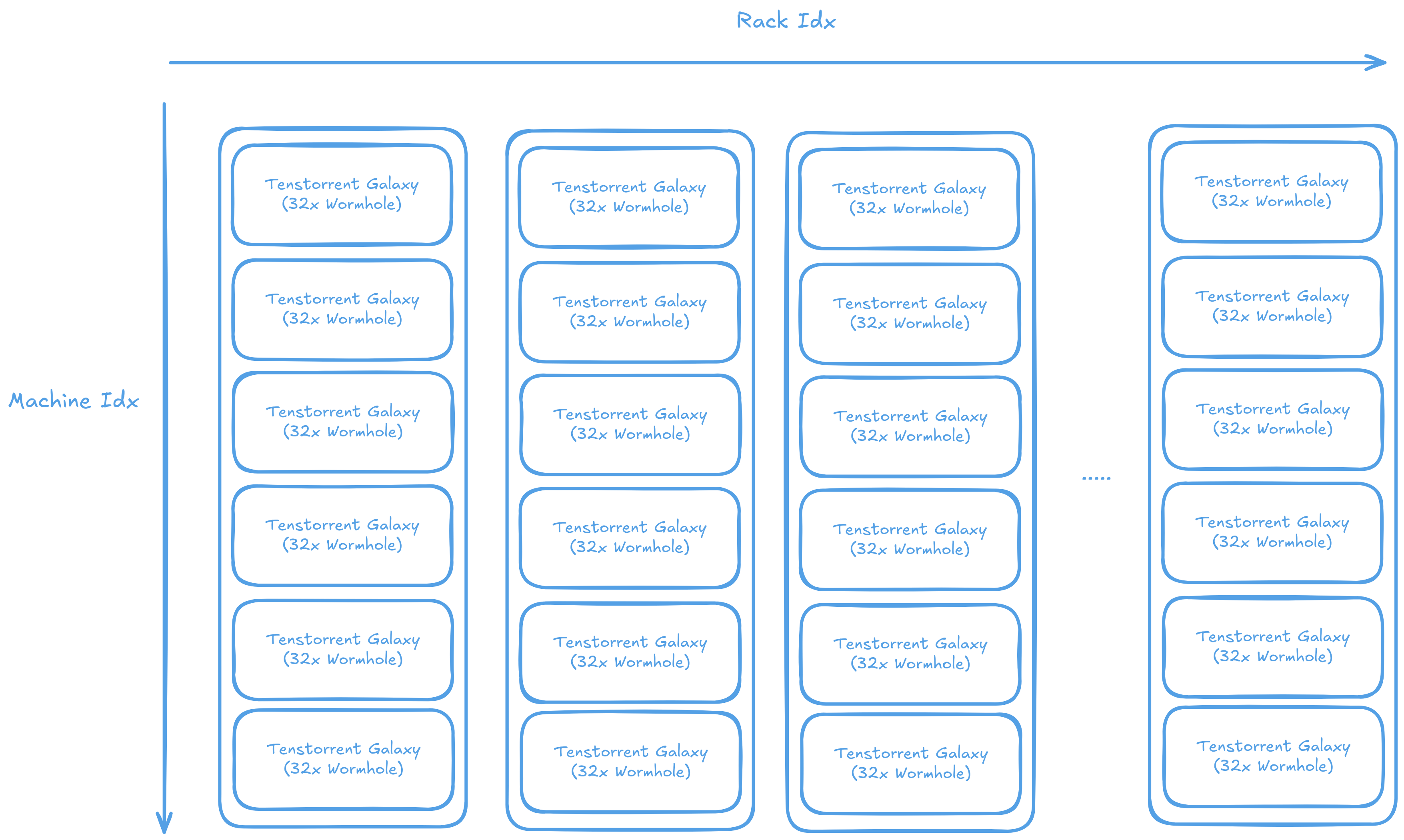
8 chips is still not that much if the end goal is to support training of the largest models. We need more connections! No worries, the exact same scheme can scale to something like 32 chips attached to a single host. And to multiple hosts with Wormhole processors connected in the same mesh.
tt-Metalium
tt-Metalium, often abbreviated as Metalium, tt-Metal or just Metal (I avoid calling it Metal as Apple also have their Metal API) is the current preferred SDK for developing and executing computational tasks on the Tenstorrent platform. The fundamental design looks like OpenCL if you squint really, really hard. It is a C++ library that provides both high-ish and low-level interfaces for interacting with Tenstorrent AI processors. In fact, the kernel shown in the 1st section are Metalium kernels.
Metalium is where everything starts. From running a single kernel on a single core to programming an entire cluster of chips. All of Tenstorrent's libraries are built on top of Metalium. Be it TTNN, tt-MLIR or tt-Forge.
Running code on device
Metalium is like OpenCL, this is reflected in the API design. The steps involved to run code on device are as follows:
- Open a device
- Allocate memory for input and output buffers
- Upload input data to the input buffer
- Compile the data movement and compute kernels
- Allocate circular buffers to pass data between kernels
- Set runtime parameters for the kernels
- Execute the kernels
- Wait for the kernels to finish executing
- Retrieve the results from the output buffer
Let's use the same example of vector addition to illustrate how to run code on Tenstorrent processors using Metalium. However, this time instead of device side code, we will look at how to use the Metalium API.
The following code demonstrates how to set up and execute a simple vector addition operation on Tenstorrent hardware using the tt-Metalium SDK. It begins by creating a device and command queue, allocating memory buffers for input and output data, and uploading the input data to the device. Next, it compiles the necessary kernels for reading, computing, and writing data, and sets runtime arguments for these kernels. Circular buffers are created to facilitate data movement between kernels. Finally, the program is enqueued for execution, and the results are retrieved from the output buffer.
IDevice* device = CreateDevice(0);
CommandQueue& cq = device->command_queue();

size_t n_tiles = 64;
size_t buffer_size = TILE_WIDTH * TILE_HEIGHT * n_tiles * sizeof(bfloat16);
size_t page_size = TILE_WIDTH * TILE_HEIGHT * sizeof(bfloat16);
InterleavedBufferConfig config{
    .device = device,
    .size = buffer_size,
    .page_size = page_size,
    .buffer_type = BufferType::DRAM};
auto a = CreateBuffer(config);
auto b = CreateBuffer(config);
auto c = CreateBuffer(config);

EnqueueWriteBuffer(cq, a, some_data, false);
EnqueueWriteBuffer(cq, b, some_data, false);
Then kernels are created for reading, computing, and writing data. In this example, we are only going to use core (0, 0) (to make things simpler). Then arguments are set for the kernels separately.
Program program = CreateProgram();
auto reader = CreateKernel(
    program,
    "tt_metal/programming_examples/contributed/vecadd/kernels/interleaved_tile_read.cpp",
    {0, 0},
    DataMovementConfig{.processor = DataMovementProcessor::RISCV_0, .noc = NOC::RISCV_0_default});
auto writer = CreateKernel(
    program,
    "tt_metal/programming_examples/contributed/vecadd/kernels/tile_write.cpp",
    {0, 0},
    DataMovementConfig{.processor = DataMovementProcessor::RISCV_1, .noc = NOC::RISCV_1_default});
auto compute = CreateKernel(
    program,
    "tt_metal/programming_examples/contributed/vecadd/kernels/add.cpp",
    {0, 0},
    ComputeConfig{.math_approx_mode = false, .compile_args = {}, .defines = {}});
SetRuntimeArgs(program, reader, core, {a->address(), b->address(), n_tiles});
SetRuntimeArgs(program, writer, core, {c->address(), n_tiles});
SetRuntimeArgs(program, compute, core, {n_tiles});
The kernels here uses circular buffer 0, 1 and 16. There is not specific reason why these IDs are chosen, doesn't make a difference. But they are chosen to be different from each other to avoid conflicts. After circular buffer allocation the program is executed, waited upon and the result is read back.
MakeCircularBuffer(program, core, tt::c_0, 4 * tile_size, tile_size, tt::DataFormat::Float16_b);
MakeCircularBuffer(program, core, tt::c_1, 4 * tile_size, tile_size, tt::DataFormat::Float16_b);
MakeCircularBuffer(program, core, tt::c_16, 4 * tile_size, tile_size, tt::DataFormat::Float16_b);

EnqueueProgram(cq, program, true);
std::vector<uint32_t> c_data;
EnqueueReadBuffer(cq, c, c_data, true);
Low-Level Kernels (LLKs)
One special thing about Metalium kernels is the existence of LLKs. Unlike GPUs where the behavior of operations is defined by their programming language, where it is the compiler's job to figure out how to issue instructions such that the final result adheres to the abstract machine's expected behavior (Plus the SIMT nature of GPU programming abstracts a lot of details away). Metalium is more like a library that allows programmers to directly issue instructions to for maximum performance. Even though Metalium sort of allows use of a SIMT-like programming model via masking. The RISC-V core issuing instructions is not aware of that and problem arises when the matrix/vector unit changes from generation to generation. On Grayskull the vector unit is 64 elements wide and does 19bit floating point operations. It got reduced to 32 elements wide and 32bit floating point operations in the following Wormhole and Blackhole generations. Code written assuming a 64-wide vector won't work when the vector unit is suddenly 32-wide.
Solution is LLKs. By using the unpacker and packer. LLKs provides a stable API for kernel writers to write kernels and know they'll keep working in future generations. Take the sine function for example writing sin_tile in a compute kernel calls to a different implementations of it. Each optimized for the specific width and capabilities of the vector unit.
sin_tile(0); // Different implementation for sin is called when compiled for
             // different generations of Tenstorrent processors.
As shown below, the implementation for Grayskull simply shifts the range from [0, 2pi] to [-pi, pi] and uses a MacLaurin series to calculate the sine.
// tt_metal/hw/ckernels/grayskull/metal/llk_api/llk_sfpu/ckernel_sfpu_trigonometry.h
template <bool APPROXIMATION_MODE, int ITERATIONS>
inline void calculate_sine() {
    // SFPU microcode
    for (int d = 0; d < ITERATIONS; d++) {
        vFloat v = dst_reg[0];

        // Assume v is bound [0:2pi]
        // phase shift [0:2pi] to [-pi:pi] and multiply result by -1
        v = v - 3.14159264f;
        v = sfpu_sine_maclaurin_series<APPROXIMATION_MODE>(v);

        // Use symmetrical properties of trig
        v *= -1;

        // Write Output
        dst_reg[0] = v;
        dst_reg++;
    }
}
On Blackhole (and Wormhole) due to having support for float_to_int16 the value can be shifted to [-pi, pi] reliably. Then again a MacLaurin series is used to calculate the sine (it's the same function but with a different name). Also ITERATIONS is different. On Grayskull it's 4 while on Wormhole/Blackhole it's 8 due to the halfed vector width.
// tt_metal/hw/ckernels/blackhole/metal/llk_api/llk_sfpu/ckernel_sfpu_trigonometry.h
template <bool APPROXIMATION_MODE, int ITERATIONS>
inline void calculate_sine() {
    // SFPU microcode
    for (int d = 0; d < ITERATIONS; d++) {
        vFloat v = dst_reg[0] * FRAC_1_PI;
        vInt whole_v = float_to_int16(v, 0);
        v -= int32_to_float(whole_v, 0);
        v = sfpu_sinpi<APPROXIMATION_MODE>(v);

        v_if(whole_v & 1) { v = -v; }
        v_endif;
        dst_reg[0] = v;
        dst_reg++;
    }
}
Writing you own vectorized computation is supported as a part of Metalium. But be aware that vector width and other details may change in future generations. Unless necessary, it's recommended to use the provided LLKs within the kernel library. Which Tenstorrent will maintain and ensure compatibility with future hardware. Please refer to the "Low Level Kernels" section in the Metalium documentation for writing your own vectorized computation.
Fast dispatch
Fast dispatch is just the fancy word for a command queue. Unlike GPUs where there's a dedicated scheduler on chip to dispatch workload and the command queue is a part of the GPU-host runtime. Tenstorrent sacrifices one RISC-V core on the chip per command queue to process the commands. Usually this runs on one of the unconnected Ethernet tiles so overall performance is not affected (remember all cores has access to all other cores?).
Without fast dispatch (can be disabled by setting TT_METAL_SLOW_DISPATCH_MODE to 1) the entire asynchronous dispatch mechanism is disabled. No command queues and no async IO from and to the host. The CPU must wait for operations to complete before proceeding. For instance, instead of EnqueueReadBuffer, ReadFromBuffer has to be used in slow dispatch mode.
// Fast dispatch. Can be async or the process waits until completion
EnqueueReadBuffer(queue, buffer, host_ptr, /*async=*/false);

// Slow dispatch. No queue. But also CPU has to do all the job
ReadFromBuffer(buffer, host_ptr);
Unlike OpenCL's command queue optionally supporting out-of-order execution, Tenstorrent's command queue is strictly in-order. However, to enable overlapping computation and data transfer, each device have 2 command queues. Queue 0 is used for computation and queue 1 is used for data transfer. An event can be obtained from one queue to wait for completion of the other queue's operations, to avoid reading from buffer that the other queue is working on computation.
TTNN
Being able to program the processor itself is good n all. But the main purpose of Tenstorrent processors is to run AI workloads. TTNN is Tenstorrent's Neural Network operator library as well as the tensor library, built on top on Metalium. TTNN provides a PyTorch-like API for both Python and C++ - all be it with some processor details leaking through the abstraction. Mainly, most operations needs to be tilzied in order for computation to be performed on them. The following performs addition in TTNN/Python. Note the use of bfloat16. Though the vector engine on Wormhole and Blackhole supports IEEE 754 32 bit floating point numbers, the matrix unit doesn't and bfloat16 is good enough for most AI workloads.
import torch
import ttnn

device = ttnn.open_device(device_id=0)
a = torch.rand((64, 64), device=device)
b = torch.rand((64, 64), device=device)

# Upload tensor from host to device, and convert into the tiled layout. DITTO for NumPy
x = ttnn.from_torch(a, dtype=ttnn.BFLOAT16, device=device, layout=ttnn.TILE)
y = ttnn.from_torch(b, dtype=ttnn.BFLOAT16, device=device, layout=ttnn.TILE)
z = ttnn.add(x, y)

# Download tensor from device to host, and convert into the PyTorch layout
z = ttnn.to_torch(z, dtype=torch.float32)
print(z)
The leaky abstractions
Ideally, abstractions should be seamless—they should hide the underlying complexity and provide developers with an intuitive interface. However, in high-performance computing, especially on specialized hardware like Tenstorrent processors, abstractions must strike a careful balance. They need to simplify development while still exposing enough of the hardware's unique capabilities to allow developers to fully utilize its potential and avoid common pitfalls. This is where TTNN's abstractions come into play. While they aim to deliver a PyTorch-like experience, certain hardware-specific details, such as tiled layouts and explicit memory management, inevitably surface. These "leaky abstractions" are a trade-off, ensuring developers can achieve optimal performance while still benefiting from a higher-level API.
Because of Metalium's programming model and its reliance on tiled processing, TTNN cannot fully replicate PyTorch's API without introducing performance compromises. Instead, it finds a middle ground by exposing hardware-specific details when necessary. The following example demonstrates what happens internally when you call ttnn.from_torch and ttnn.to_torch.
torch_tensor = torch.randn(3, 3, dtype=torch.float32)

a = ttnn.from_torch(torch_tensor)    # Create a TTNN tensor from a PyTorch tensor with data type
                                     # inferred from the PyTorch tensor type. By default this is
                                     # in the classic row-major layout and lives on the host memory

b = a.to_device(device)              # Move the tensor to the device, still in row-major layout

c = ttnn.tilize_with_zero_padding(b) # As now tensor is on the device, we can invoke ttnn
                                     # tilize_with_zero_padding to convert the tensor to a tiled layout

# At this point `c` is in the expected format TTNN can use for computation

d = ttnn.untilize(c)                 # Convert the tiled tensor back to a row-major layout
e = d.cpu()                          # Convert the tensor back to the host memory

result_torch = e.to_torch()          # Convert the tensor to a PyTorch tensor
The "view" class of operations, including slice, view, transpose, and permute are a light weight powerful tool for changing the order of how a tensor is read. They rely on the fact that tensors are stored in contiguous memory, allowing for efficient memory access patterns. The tiled layout of Tenstorrent devices does not permit such operations directly. Since a tile is 32x32 on Tenstorrent devices, view on the last 2 dimensions often leads to real memory reordering, instead of just changing the strides. Thus the operations may be much slower then expected on a GPU, as they require additional memory transfers and computations. For example
a = torch.randn((768, 42))
x = ttnn.from_torch(a, layour=ttnn.TILE, device=device, dtype=ttnn.BFLOAT16)

b = torch.transpose(a, 0, 1) # virtually free until the transposes needs to be resolved (if ever needed)
y = ttnn.transpose(x, 0, 1) # Very slow as a real transpose is performed

c = a[12:68, :] # Again virtually free until realizing the slice is ever needed
z = x[64:128, :] # Expensive! TTNN has actually copy the memory

c[0, :] = 0 # Works because views are lazy and we can write into a view
z[0, :] = 0 # Does not work. TTNN always copies the memory so the reference is lost

# However if you mess with non-tilzed dimensions. Things are fine now
a = torch.randn(64, 64, 32, 32)
x = ttnn.from_torch(a, layout=ttnn.TILE, device=device, dtype=ttnn.BFLOAT16)

b = torch.permute(a, (1, 0, 2, 3)) # Works as expected
y = ttnn.permute(x, (1, 0, 2, 3)) # Also fast because only the last 2 dimensions are tiled
Care also has to be taken when using SRAM in Python. SRAM is a very limited resource while the Python GC may run at unpredictable times - SRAM may not be released in time for the next operation needing it leading to OOM. To avoid this, it is recommended to use the tensor.deallocate() function to release the memory when it is no longer needed.
d = ttnn.matmul(x, y, memory_config=ttnn.L1_MEMORY_CONFIG) # Put the result in L1 (SRAM)
e = ttnn.multiply(c, d)
d.deallocate() # Release the memory used by d otherwise it hogs SRAM until Python GC runs
Collective Communications Library (CCL)
The programming model of Tenstorrent devices is uniform and scalable. But that does not excuse it from being bottlenecked by the chip-to-chip interconnect bandwidth and NUNA limitations. Ideally, even under multi chip settings. Processors should only access memory that is local to them; less saturating the interconnect immediately. Only when needed, data should be transferred between processors. This is where CCL comes into play. CCL is an efficient implementation of operations that involves communication between processors.
Nvidia's NCCL (Nvidia Collective Communication Library) has a great document on what CCL operations do
In TTNN, CCL is a part of the overall design, instead of being a separate library. CCLs can be directly called from TTNN.
.... # Some complex code
z = do_some_computation()

# Reduce the tensor across all processors. Now all processors (physically) store the same value
reduced = ttnn.all_reduce(z)

# Broadcast the tensor from one processor to all others
broadcasted = ttnn.broadcast(z)
That's it. Hope it helps you.