The Real Tenstorrent Tensix Programming Model (FOSDEM 2026 draft)
Weird timing. I left Tenstorrent at this point, but I still have a talk at FOSDEM about Tenstorrent and the processor. Because that's fun. Luckily my new employer still allows me to talk about it - so in my tradition, here's the draft!
The talk is "All in RISC-V, RISC-V All in AI: Solving Real AI Compute Challenges". I'm sharing the stage with DeepComputing because they have some fun ideas, and I had the last time to myself. This year I could use some rest. The title is more of a misnomer. What I actually want to share is what really hides under the hood and how by understanding it performance can be improved. Consider this a "How does a specific aspect of Tenstorrent chip work" talk. And if anyone wants to say "I can learn this by Google, duh" -- I am the reason you can Google this at all.
The talk will largely pull experience from my RoPE post as reference material, since that post covers a lot of the core ideas and details.
Also I truly respect Felix and his philosophy about processors. But this talk is going to kill him.
The Tensix Processor design
Any processor architecture has to be designed to solve something. That something for Tenstorrent is to run AI (both Conv nets and Transformers) well within power and chip area constraints. But that's the problem every AI chip company is trying to solve - be it AMD, Intel, Google, Groq or heck, even Nvidia. The specific bet Tenstorrent is going with is this: instead of adding hardware that takes up area and power to solve some architecture inefficiencies, why not just stick RISC-V cores everywhere? Memory? RISC-V. Compute? RISC-V. Core to core comms? RISC-V. Chip to chip? Yes, also RISC-V.
This design philosophy means the processor is logically (and semi-physically) organized as a grid of cores.

The most generic way to program the processor is the same as every (sane) processor out there: SPMD. There are 64 cores on a WH chip on N150. Simply make the cores handle part of the input tensor and call it a day. While this approach is generic and broadly applicable, it's not the most efficient way to do things for all operations.
The most critical and compute-intensive operations in modern AI workloads are matrix multiplication, attention, and convolution. I might refer to matrix multiplication as GEMM later on - they are the same thing, but GEMM is shorter and widely used in HPC.
Since the Tensix cores are logically arranged into a grid, classic literature on systolic arrays is very applicable.
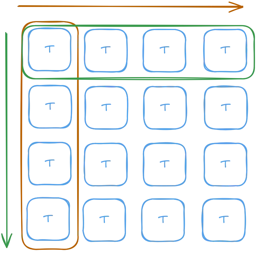
But these Tensix cores are more flexible than your classic systolic array. For GEMV (matrix-vector multiplication), we can do better by only loading the vector once and then broadcasting it to rows/columns, followed by a ring-reduce to compute the final result - drastically cutting down the total consumed memory bandwidth. Sure you can do that with systolic arrays, but unless you explicitly built that in while you are working on the HDL, or you are on FPGA only, you really need a galaxy brain to have the foresight to do that. With programmable cores, that's straightforward and can always be implemented later on (with software performance penalties, but better than impossible).

The same flexibility applies to convolutions. While you can make systolic arrays do convolution, that state machine to coordinate the PEs is practically a pain to build and hard to generalize to different kernel sizes and channel depths (been there, done that). It is much easier and faster putting things in software and letting the kernel programmer handle that directly - assuming the main bottleneck is going to be the matrix engine within the Tensix, not the control logic.
The following diagram shows that convolution only needs the Tensix cores themselves accessing data next to them physically. This setup is much more efficient than GPUs managing core-to-core communications over the L2 cache and the crossbar.

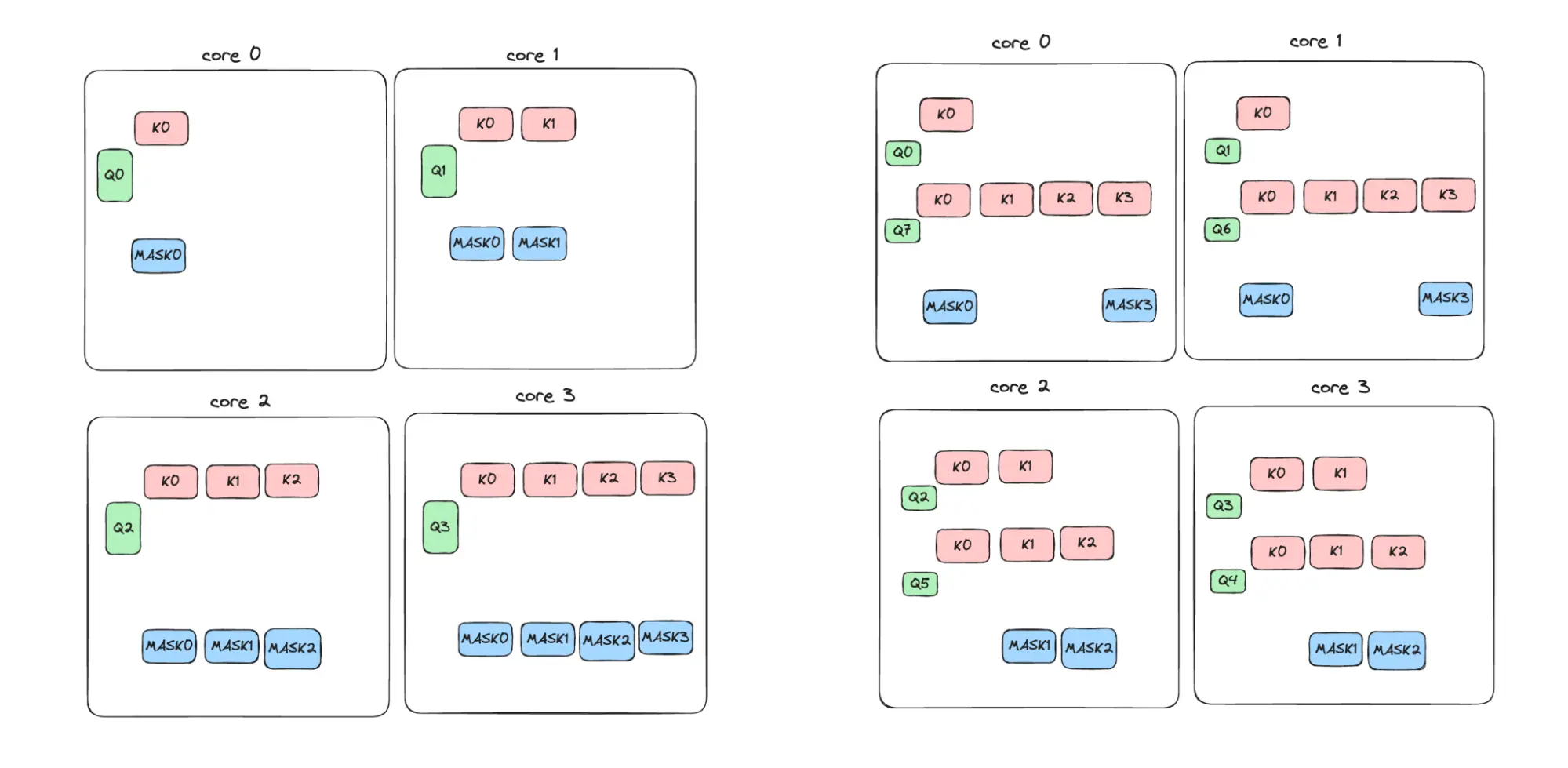
The same pattern holds for attention - though that diagram is too complicated so I'll steal one from the repository (it's Apache 2.0 anyway).
The (Tensix) core design
So how do these Tensix cores work internally? Unfortunately, the "core" name is really a misnomer and they only look like a core if you squint really hard and think abstractly. In reality, the Tensix cores are actually a collection of high-performance peripherals controlled by 5 independent "Baby" RISC-V cores - these baby cores look more like a MIPS R3000 in design than even smaller cores like Intel's Knights Landing or Silvermont. The baby cores only support the RISC-V IM instruction set with some Tenstorrent-specific extensions to control the peripherals.

The 5 RISC-V cores are labeled Data Movement 0, Data Movement 1, UNPACK, MATH, and PACK respectively. In the Metalium programming model, the DM0 and DM1 cores run independent data movement kernels to bring in data for computation from DRAM or local SRAM of other devices. Meanwhile, UNPACK, MATH, and PACK run a singular computation kernel - the runtime, through some macro magic, automatically splits and assigns each core to a different part of the computation pipeline.
Wait... how does that work? What the actual f.....k? How does the runtime split work based on macro magic on arbitrary code? How exactly?
Let's read some actual code to understand this better. DM0 and DM1 are easy. Essentially what they do is say "here's the address and tensor metadata (SRAM/DRAM, etc.) I wish to read from and here's the size. Wait for space in pipe #0 then read and push into it". Writing works the same but in reverse. This part should be trivial after reading the Metalium docs.
// Reader (DM0)
void kernel_main() {
    uint32_t in0_addr = get_arg_val<uint32_t>(0);
    uint32_t n_tiles = get_arg_val<uint32_t>(1);

    constexpr uint32_t cb_in0 = tt::CBIndex::c_0;

    constexpr auto in0_args = TensorAccessorArgs<0>();
    const auto in0 = TensorAccessor(in0_args, in0_addr, get_tile_size(cb_in0));

    for (uint32_t i = 0; i < n_tiles; i++) {
        cb_reserve_back(cb_in0, 1);
        uint32_t cb_in0_addr = get_write_ptr(cb_in0);
        noc_async_read_tile(i, in0, cb_in0_addr);

        noc_async_read_barrier();
        cb_push_back(cb_in0, 1);
    }
}

// Writer (DM1)
void kernel_main() {
    uint32_t c_addr = get_arg_val<uint32_t>(0);
    uint32_t n_tiles = get_arg_val<uint32_t>(1);

    constexpr uint32_t cb_out0 = tt::CBIndex::c_16;

    constexpr auto out0_args = TensorAccessorArgs<0>();
    const auto out0 = TensorAccessor(out0_args, c_addr, get_tile_size(cb_out0));

    for (uint32_t i = 0; i < n_tiles; i++) {
        cb_wait_front(cb_out0, 1);
        uint32_t cb_out0_addr = get_read_ptr(cb_out0);
        noc_async_write_tile(i, out0, cb_out0_addr);
        noc_async_write_barrier();
        cb_pop_front(cb_out0, 1);
    }
}
The compute kernel looks funny. namespace NAMESPACE { void MAIN {? Also what's with the manual managing of registers? What register? And why are there synchronization mechanisms within what's supposedly a single core? While we could just accept it as-is and copy and paste, we are hackers aren't we? Let's dig a bit deeper.
namespace NAMESPACE {
void MAIN {
    uint32_t n_tiles = get_arg_val<uint32_t>(0);

    // Initialize the SFPU
    init_sfpu(tt::CBIndex::c_0, tt::CBIndex::c_16);
    exp_tile_init();
    for (uint32_t i = 0; i < n_tiles; i++) {
        cb_wait_front(tt::CBIndex::c_0, 1);
        // Make sure and acquire data before running the SFPU operation
        tile_regs_acquire();
        // Copy the tile from the circular buffer offset 0 to the tile registers 0
        copy_tile(tt::CBIndex::c_0, /*offset*/ 0, /*register_offset*/ 0);

        // Invoke the SFPU exponential operation on tile 0
        exp_tile(0);
        tile_regs_commit();
        tile_regs_wait();

        // Clean up and prepare for the next iteration
        cb_reserve_back(tt::CBIndex::c_16, 1);
        pack_tile(0, tt::CBIndex::c_16);  // copy tile 0 from the registers to the CB
        cb_pop_front(tt::CBIndex::c_0, 1);
        tile_regs_release();
        cb_push_back(tt::CBIndex::c_16, 1);
    }
}
}
Like I said, the compute side of the Tensix is not a monolithic thing. This shows up most prominently in that the actual vector and matrix math engines DO NOT have direct access to the SRAM scratch pad where the data movement kernels load data into. Data must be unpacked into BFloat16 or FP32 in order to be consumed by the math engines. Likewise, the math engines don't produce the compressed/quantized formats that Metalium supports. That's the packer's job - to pack BFloat16 or FP32 into BFLOAT8/4.
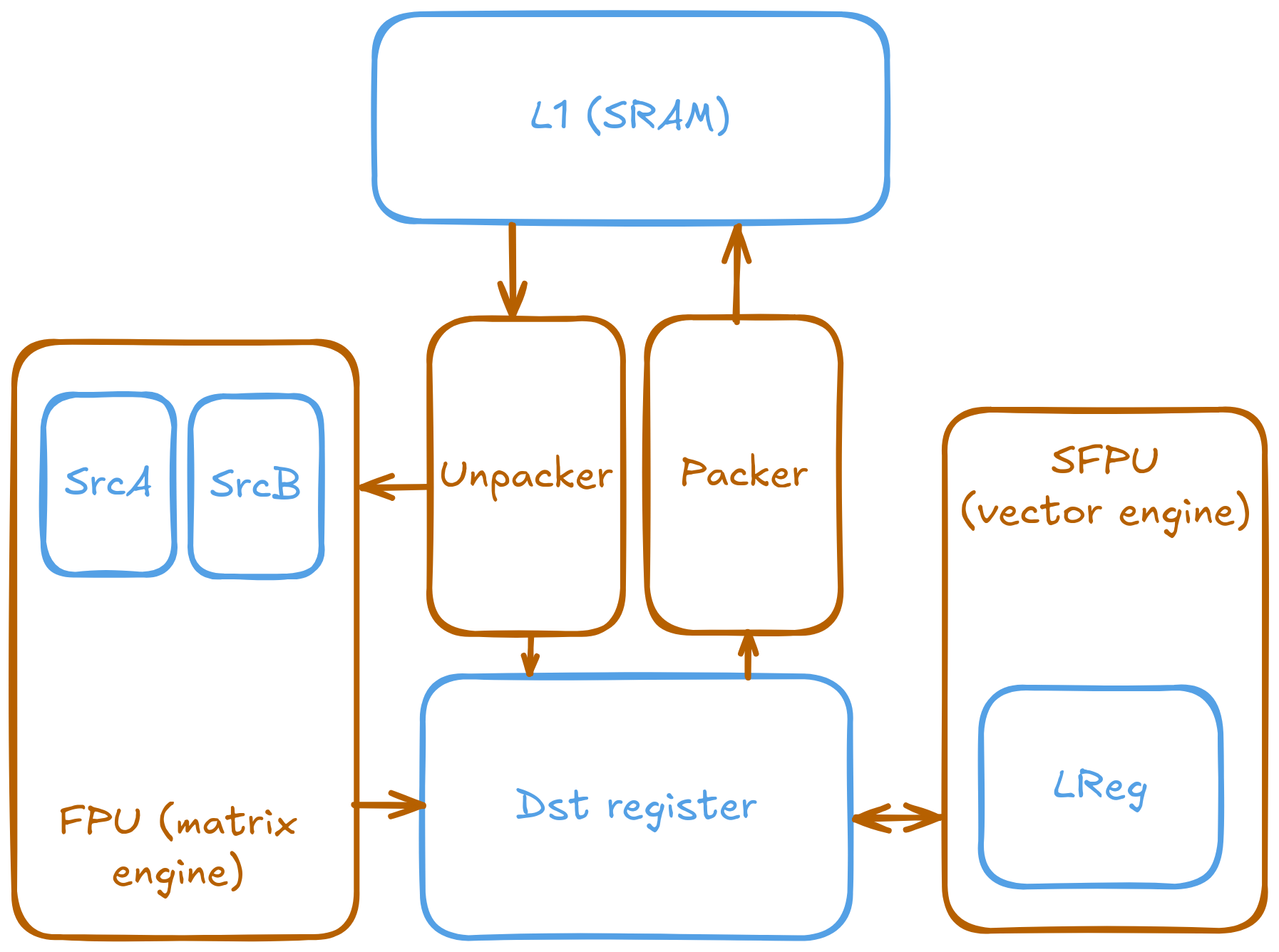
To understand what exactly the compute kernel is doing, we must understand what the Dst registers are. You can find official documents in the following link. But don't click on it just yet... I wrote it so this post is as valid as the official document.
The name "Dst" is yet another misnomer with a historical origin - it was originally the destination of the matrix engine (FPU). However, Tenstorrent engineers realized later on that models started needing activation functions beyond (leaky-)ReLU and sigmoid. Plus precisions started to matter more and more in certain parts of computations (and covering them with softfp is not a viable path). The SFPU was then born. But where to add it? Since it's mostly going to be dealing with activations, it's easier to just bolt it onto Dst. Hence now DST is both a destination and a source register.
Programmatically the Dst can be understood as 16 tiles of BFP16 or 8 tiles of FP32, with half of it being usable at each time - double buffered to allow the math engine to run while the unpacker is unpacking data for the next loop iteration.
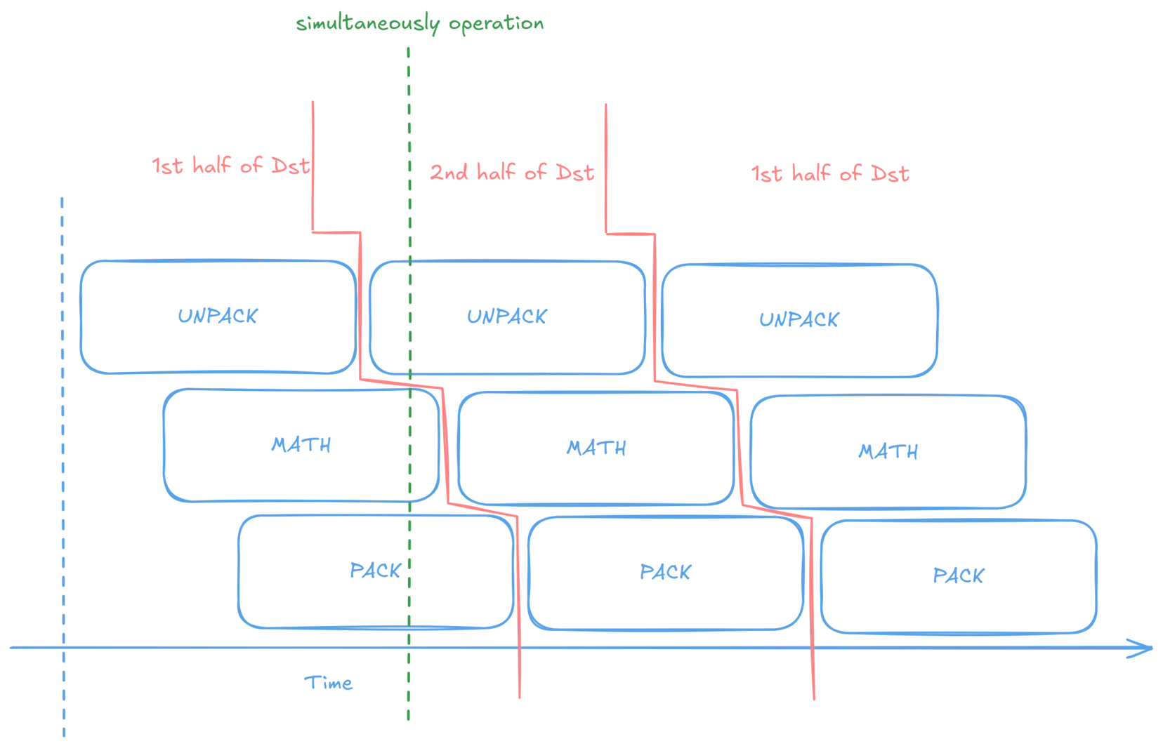
Now let's revisit the synchronization mechanism. The typical structure of computation is as follows:
tile_regs_acquire();

// unpack to dst and do math here

tile_regs_commit();
tile_regs_wait();

// pack data to sram here

tile_regs_release();
tile_regs_acquire() does the synchronization between cores, making sure at least one of the Dst halves is available for both the unpack and math cores (important: due to hardware constraints, moving data from SRAM to DST needs both cores driving the unpacker and FPU at the same time). tile_regs_{commit,wait} then ensures the packer has full access to the DST register, without interference from unpacker and math. Finally, tile_regs_release() releases the DST register for future use.
Let me use the following meme to share how I feel after I finally understood how this all works.

This fact is abusable - as we now know the Dst registers are not touched by random unpredictable threads. If you ever have expensive computation, it is totally safe to just put that in one of the Dst registers, twice. Then you can ignore the expensive computation in future iterations.
for (uint32_t i = 0; i < n_tiles; i++) {
    // double buffered: i.e. we only need to set up twice
    if(i < 2)
        some_expensive_one_time_computation(/*output_reg=*/0);

    add_tiles(...);
}
Back to the actual computation - exp_tile_init() sets programmable constant registers - global variables within the vector unit themselves. As loading floating point values, even if constant, takes 2 cycles. While referencing constants already loaded is 0 latency. Unfortunately, this optimization makes SFPU operations rather stateful - whatever xxx_tile() must be preceded by xxx_tile_init() to set up the correct internal state.
inline void _init_sfpu_reciprocal_()
{
    vConstFloatPrgm0 = 0.3232325017452239990234375f;
    vConstFloatPrgm1 = 1.4545459747314453125f;
    vConstFloatPrgm2 = 2.121212482452392578125f;
}
Then exp_tile() eventually invokes the actual computation of exponents. Notice the v_* statements. These work slightly different to your regular C++ if. These work by predicating vector lanes, exactly like how early GPUs work. There is no early branch termination and C++ statements within the blocks are always executed. Be wary about the performance drag from having 2 large possible paths - both paths are always taken. Programming the SFPU feels like programming GPU without SIMT abstracting the underlying parallelism.
vFloat val = sfpi::dst_reg[0];

....
v_if(z >= OVERFLOW_THRESHOLD) {
    // Overflow
    result = std::numeric_limits<float>::infinity();
}
v_elseif(z <= UNDERFLOW_THRESHOLD) {
    // Underflow
    result = sfpi::vConst0;
}
v_else {
    // Round z to nearest integer using round-to-nearest-even
    sfpi::vInt k_int;
    sfpi::vFloat k = _sfpu_round_nearest_int32_(z, k_int);
    ....
}
v_endif;

...

dst_reg[0] = result;
dst_reg++;
SFPU
The SFPU contains a macro recording and expansion unit. It is responsible for issuing repeated instructions (in a loop) while the driving baby core is running the loop body logic - as compensation for the baby core being only capable of 1 instruction per cycle. During execution of a macro, the SFPU and the baby core essentially run in parallel and no communication can be done between them.
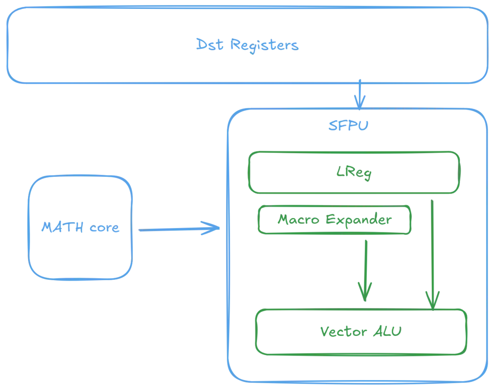
This explains the common pattern in the SFPU code to use dst_reg++ instead of using the loop counter for index advancement. Incrementing the dst register index allows the compiler to generate pure SFPU code that can be macro-ed to effectively hide the looping overhead.
#pragma unroll 0
for (uint32_t i = 0; i < n_tiles; i++) {
    vFloat y = ckernels::sin(dst_reg[0]);
    dst_reg[0] = y;
    dst_reg++;
}
Later on, a stall is issued to ensure the SFPU has finished execution and data is available to the packer.
TTI_STALLWAIT(p_stall::STALL_CFG, p_stall::WAIT_SFPU);
Here we go again.

Argghhh!!!!!!! (/‵Д′)/~ ╧╧
It is dataflow machines all the way down. Everything is asynchronous. Efficiency can be squeezed from running control flow while the engines are busy doing math. But it's also different - different enough that programming needs a completely different mindset. Or pipelines